Hirokawa delivers transmission solutions for a wide range of semiconductor process equipment
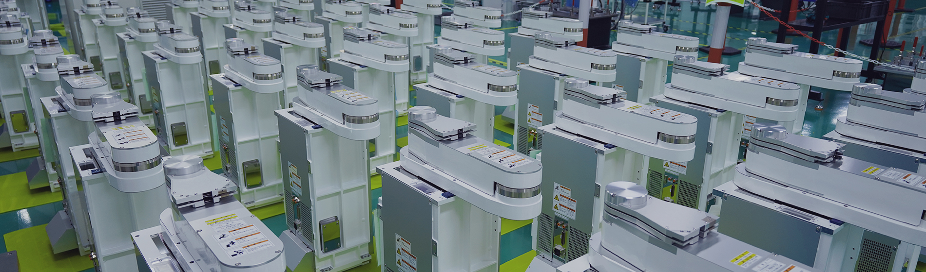

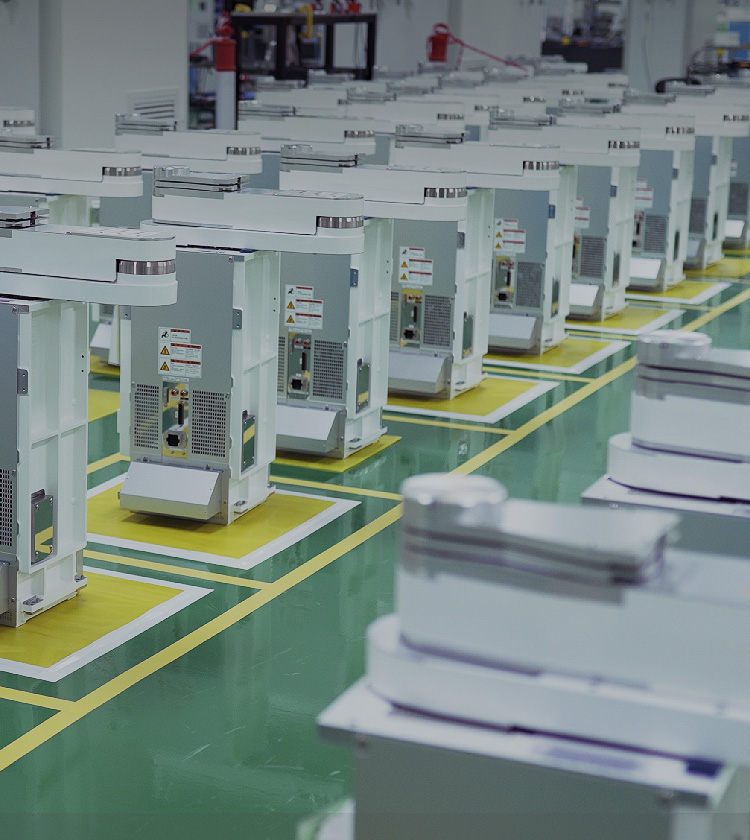


In semiconductor processes, whether in Atmospheric Environment, Vacuum Environment, EFEM side, or PROCESS side, mature transfer solutions are available, committed to providing clean, efficient, and stable equipment transfer products for domestic semiconductors.
| Product | Item | Specification | ||
|---|---|---|---|---|
| EFEM | Applicable wafer dimensions | 300mm(200mm) | ||
| Wafer transfer methods | Edge gripping / vacuum adsorption / Passive friction | |||
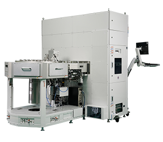
| Product type | 2Port EFEM | 3Port EFEM | 4Port EFEM | |
| Dimensions and appearance | W1600*D820 (+451) *H2200mm | W2100*D820 (+451) *H2200mm | W2600*D820 (+451) *H2200mm | |
| Number of Ports | 2 | 3 | 4 | |
| Transfer chamber | Temperature resistance | 20°~700° | ||
| Processing surface | Anodizing (internal and external), bare aluminum, multiple surface treatments | |||
| Vacuum pump | Dry pump, molecular pump | |||
| Transfer accuracy | ≤0.1mm | |||
| Vacuum performance | 1E-9Torr | |||
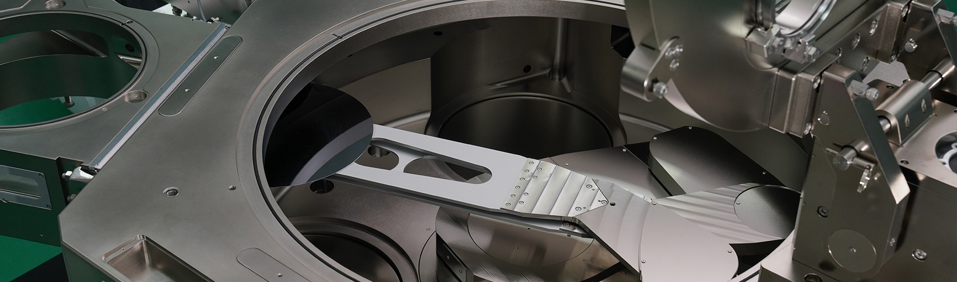
| Vacuum Robot | Model | GVM3HDA | ||
| End Effector | Ceramic, quartz, aluminum | |||
| AWC | 200mm/300mm support | |||
| Load Lock | Quantity | 1~2 | ||
| Slot | 1~27 | |||
| cooling | Optional configuration | |||